

 ics@suntelecom.cn
 +86 21 60138638
 suntelecom.s01
 +86 21 6013 8637


Para que sientas una mejor experiencia en nuestro sitio web, te recomendamos que actualizes el navegador Internet Explorer a la última versión o seleccione otros navegadores para acceder a nuestro sitio web.
Puede descargar en el navegador principal:

Google Chrome

Firefox

IE11
 Posición:
La página inicial >
Productos
> Componentes Activos
> Transceptores Ópticos
Posición:
La página inicial >
Productos
> Componentes Activos
> Transceptores Ópticos
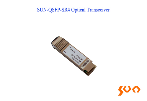
40G QSFP+Optical Transceiver, suitable for mutilmode OM3 Max distance 100m, OM4 Max 150m.

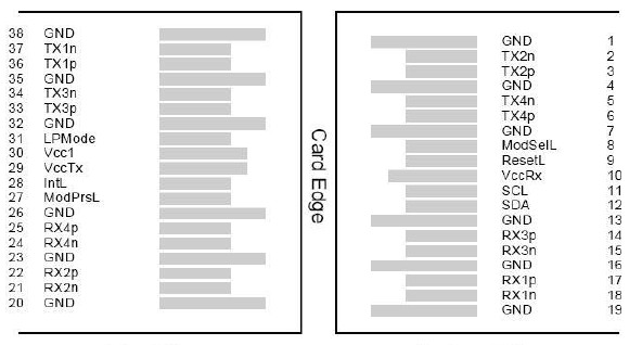
| PIN | Logic | Symbol | Name/Description | Notes |
| 1 | GND | Ground | 1 | |
| 2 | CML-I | Tx2- | Transmitter Inverted Data Input | |
| 3 | CML-I | Tx2+ | Transmitter Non-Inverted Data Input | |
| 4 | GND | Ground | 1 | |
| 5 | CML-I | Tx4- | Transmitter Inverted Data Input | |
| 6 | CML-I | Tx4+ | Transmitter Non-Inverted Data Input | |
| 7 | GND | Ground | 1 | |
| 8 | LVTLL-I | MODSEIL | Module Select | 2 |
| 9 | LVTLL-I | ResetL | Module Reset | 2 |
| 10 | VccRx | +3.3V Power Supply Receiver | ||
| 11 | LVCMOS-I/O | SCL | 2-Wire Serial Interface Clock | 2 |
| 12 | LVCMOS-I/O | SDA | 2-Wire Serial Interface Data | 2 |
| 13 | GND | Ground | 1 | |
| 14 | CML-O | Rx3+ | Receiver Non-Inverted Data Output | |
| 15 | CML-O | Rx3- | Receiver Inverted Data Output | |
| 16 | GND | Ground | 1 | |
| 17 | CML-O | Rx1+ | Receiver Non-Inverted Data Output | |
| 18 | CML-O | Rx1- | Receiver Inverted Data Output | |
| 19 | GND | Ground | 1 | |
| 20 | GND | Ground | 1 | |
| 21 | CML-O | Rx2- | Receiver Inverted Data Output | |
| 22 | CML-O | Rx2+ | Receiver Non-Inverted Data Output | |
| 23 | GND | Ground | 1 | |
| 24 | CML-O | Rx4- | Receiver Inverted Data Output | 1 |
| 25 | CML-O | Rx4+ | Receiver Non-Inverted Data Output | |
| 26 | GND | Ground | 1 | |
| 27 | LVTTL-O | ModPrsL | Module Present | |
| 28 | LVTTL-O | IntL | Interrupt | 2 |
| 29 | VccTx | +3.3 V Power Supply Transmitter | ||
| 30 | Vcc1 | +3.3 V Power Supply | ||
| 31 | LVTTL-I | LPMode | Low Power Mode | 2 |
| 32 | GND | Ground | 1 | |
| 33 | CML-I | Tx3+ | Transmitter Non-Inverted Data Input | |
| 34 | CML-I | Tx3- | Transmitter Inverted Data Input | |
| 35 | GND | Ground | 1 | |
| 36 | CML-I | Tx1+ | Transmitter Non-Inverted Data Input | |
| 37 | CML-I | Tx1- | Transmitter Inverted Data Input | |
| 38 | GND | Ground | 1 |
| Parameter | Symbol | Min | Max | Units |
| Storage Temperature | Tst | -20 | 85 | ºC |
| Input Voltage | Vin | -0.3 | Vcc+0.3 | V |
| Power Supply Voltage | Vcc | -0.3 | 3.6 | V |
| Relative Humidity (non-condensation) | RH | 5 | 95 | % |
| Parameter | Symbol | Min | Typical | Max | Units | |
| Operating Temperature | Non-industrial | Tc | 0 | 70 | ºC | |
| Industrial | Tc | -40 | 85 | ºC | ||
| Power Supply Voltage | Vcc | 3.13 | 3.3 | 3.47 | V | |
| Date Rate Each Lane | fd | 10.3 | 10.5(1) | Gbps | ||
| Power Dissipation | Pm | 1.5 | W | |||
| Fiber Bend Radius | Rb | 3 | CM | |||
| Parameter | Symbol | Min | Typical | Max | Units |
| Differential Input Impedance | Zin | 90 | 100 | 110 | Ohm |
| Differential Output Impedance | Zout | 90 | 100 | 110 | Ohm |
| Differential Input Voltage Amplitude | ΔVin | 300 | 1100 | mVp-p | |
| Differential Output Voltage Amplitude | ΔVOut | 500 | 800 | mVp-p | |
| Skew | Sw | 300 | ps | ||
| Bit Error Rate | BER | E-12 | |||
| Input Logic Level High | VIH | 2 | VCC | V | |
| Input Logic Level Low | VIL | 0 | 0.8 | V | |
| Output Logic Level High | VOH | VCC-0.5 | VCC | V | |
| Output Logic Level Low | VOL | 0 | 0.4 | V |
| Parameter | Symbol | Min | Typical | Max | Units | Notes |
| Transmitter | ||||||
| Center Wavelength | λC | 840 | 850 | 860 | nm | |
| RMS Spectral Width | ∆λ | 0.65 | nm | |||
| Average Launch Power Each Lane | Pavg | -7.5 | 2.5 | dBm | ||
| Difference in Launch Power between any Two Lanes (OMA) |
4 | dBm | ||||
| Extinction Ratio | ER | 3 | dB | |||
| Peak Power Each Lane | 4 | dBm | ||||
| Transmitter and Dispersion Penalty (TDP) Each Lane |
TDP | 3.5 | dB | |||
| Transmitter Eye Mask Definition {X1, X2, X3, Y1, Y2, Y3} | {0.23, 0.34, 0.43, 0.27, 0.35, 0.4} | Hit Ratio = 5x10⁻⁵ | ||||
| Average Launch Power OFF Transmitter Each Lane | -30 | dB | ||||
| Receiver | ||||||
| Center Wavelength | λC | 840 | 850 | 860 | Nm | |
| Minimum Average Received Power Each Lane | -9.5 | dBm | ||||
| Receiver Reflectance | Rr | -12 | dB | |||
| Maximum Average Received Power Each Lane | 2.4 | dBm | ||||
| Stressed Receiver Sensitivity (OMA) Each Lane | -5.4 | dBm | 1 | |||
| Peak Power Each Lane | 4 | dBm | ||||
| LOS Assert | LOSA | -30 | dBm | |||
| LOS De-Assert-OMA | LOSD | -7.5 | dBm | |||
| LOS Hysteresis | LOSH | 0.5 | dB | |||
| Model | Name | Description |
| SUN-QSFP-40G-SR4 | Optical Transceiver | QSFP+ SR4, 40Gbps; 100m on OM3 fiber and 150m on OM4 fiber; Non-industrial grade |
| SUN-QSFP-40G-SR4-I | Optical Transceiver | QSFP+ SR4, 40Gbps; 100m on OM3 fiber and 150m on OM4 fiber; Industrial grade |
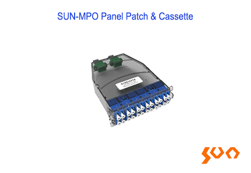
SUN-MPO Panel Patch & Cassette
Modelo: SUN-MPO
19 " Standard rack structure, rack height 1U/4U, big capacity
Features
 Fácil de instalar y operar Estructura estándar de 19 pulgadas Alta densidad, gran capacidad
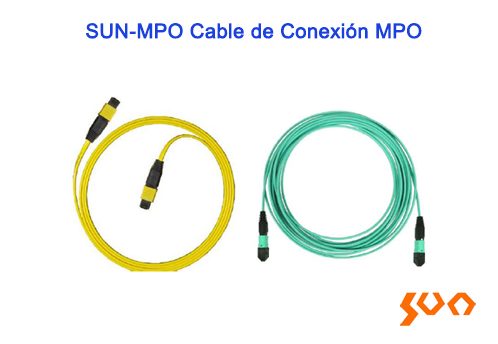
SUN-MPO Cable de Conexión MPO
Modelo: SUN-MPO
Cost-effective, time-consuming field termination, high-density fiber patching in data centers
Features
Baja pérdida de inserción Alta pérdida de retorno Buena durabilidad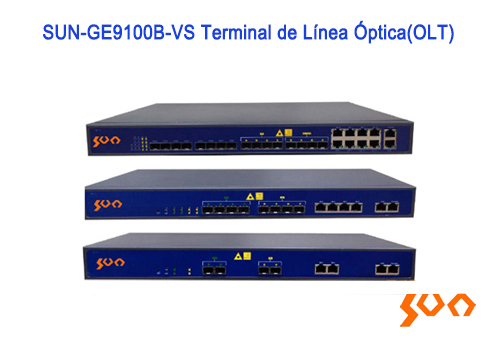
Terminal de Línea Óptica SUN-GE9100B-VS (OLT)
Modelo: SUN-GE9100B-VS
2 ⁄ 4 ⁄ 8 PON ports and connect Max 512 remote ONUs (by 1:64 splitting ratio)
Features
Ahorro de Espacio Conveniente para instalación y mantenimiento Máximo de 16×PON, 8×Gigabites de uplink óptico y puertos de uplink de bronze de 8×Gigabites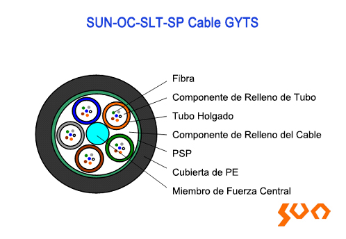
SUN-OC-SLT-SP GYTS Cable
Modelo: SUN-OC-SLT-SP
GYTS, Loose Tube Light-armored (Steel Tape) Cable, 2-144cores
Features
Buen desempeño mecánico y de temperatura Alta resistencia a la hidrólisis y tubo holgado de alta fuerza Resistencia al aplaste perfecta Alta fuerza tensil asegurada por la guaya de acero Buena resistencia a la humedad asegurada por la PSP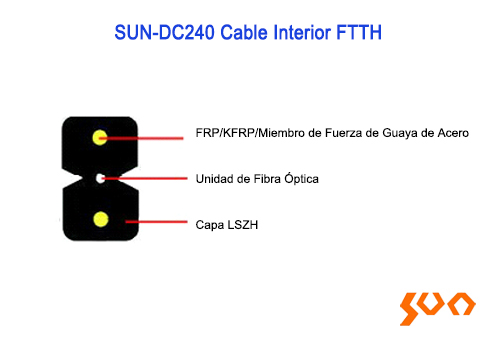
SUN-DC240 Cable Interior FTTH
Modelo: SUN-DC240
Drop Cable, 1-4 cores, G657, flame retardent, for FTTH application
Features
Buena resistencia al aplaste asegurada por miembros de fuerza paralelos Poco humo, capa sin halógeno Estructura simple, peso ligero y practicidad alta
SUN-OT5000 OTDR
Modelo: SUN-OT5000
Can test SM and MM fibers, optional light source, VFL and power meter
Features
Quick startup FTTX in-service testing (Up to1:64 splitter) Built-in PON power meter for Triple-play testing High configuration series include optical light source, optical power meter, visual fault locator (VFL) and Optical Connector Inspector (MCI) modules USB data interface (PC software for batch data processing and report output) Dustproof and shockproof (2-meter drop test) Light weight, small size, rugged design and simple operation Visual link image software (Optional)
SUN-OPM200 Optical Power Meter
Modelo: SUN-OPM200
FC ⁄ SC ⁄ ST, REF, backlight control, USB port
Features
User self-calibration function Power measurements in dBm or mW Auto power off after 10 minutes without operation Standard FC/SC/ST interchangeable port Backlight LCD display for night operation REF setting function Intelligent backlight control Auto wavelength and frequency identification High storage capacity USB communication port for data transfer
SUN-FS950-I Empalmadora de Fibra Óptica
Modelo: SUN-FS950
Backbone Type Fusion splicer
Features
Empalme de Troncal del cable de fibra óptica Alineamiento de fibra por la tecnología PAS Tiempo de empalme de 9s y 20s de calentamiento Variedad de métodos de alineamiento de fibra Monitor LCD color TFT de 5.7 pulgadas


 ics@suntelecom.cn
  +86 21 60138638
 Edificio No. 145, Vía 666 Xia Ning Road, Zona industrial de Jinshan, Shanghai, China
Copyright © "Sun Telecom" Todos los derechos reservados
ICP (Shanghai) Número: 13005159